Beranda
/ Fermi Level In Intrinsic Semiconductor Derivation : Intrinsic Semiconductor - Power Microelectronics. Device ... : E2 vf 2 ζ n(ef )ℰ for 3 dimensions:
Fermi Level In Intrinsic Semiconductor Derivation : Intrinsic Semiconductor - Power Microelectronics. Device ... : E2 vf 2 ζ n(ef )ℰ for 3 dimensions:
Insurance Gas/Electricity Loans Mortgage Attorney Lawyer Donate Conference Call Degree Credit Treatment Software Classes Recovery Trading Rehab Hosting Transfer Cord Blood Claim compensation mesothelioma mesothelioma attorney Houston car accident lawyer moreno valley can you sue a doctor for wrong diagnosis doctorate in security top online doctoral programs in business educational leadership doctoral programs online car accident doctor atlanta car accident doctor atlanta accident attorney rancho Cucamonga truck accident attorney san Antonio ONLINE BUSINESS DEGREE PROGRAMS ACCREDITED online accredited psychology degree masters degree in human resources online public administration masters degree online bitcoin merchant account bitcoin merchant services compare car insurance auto insurance troy mi seo explanation digital marketing degree floridaseo company fitness showrooms stamfordct how to work more efficiently seowordpress tips meaning of seo what is an seo what does an seo do what seo stands for best seotips google seo advice seo steps, The secure cloud-based platform for smart service delivery. Safelink is used by legal, professional and financial services to protect sensitive information, accelerate business processes and increase productivity. Use Safelink to collaborate securely with clients, colleagues and external parties. Safelink has a menu of workspace types with advanced features for dispute resolution, running deals and customised client portal creation. All data is encrypted (at rest and in transit and you retain your own encryption keys. Our titan security framework ensures your data is secure and you even have the option to choose your own data location from Channel Islands, London (UK), Dublin (EU), Australia.
Fermi Level In Intrinsic Semiconductor Derivation : Intrinsic Semiconductor - Power Microelectronics. Device ... : E2 vf 2 ζ n(ef )ℰ for 3 dimensions:. As the temperature increases free electrons and holes gets generated. For semiconductors (intrinsic), the fermi level is situated almost at the middle of the band gap. Hence, at 0k the valence band will be full of electrons while the conduction band will be empty (figure 2a). Derive the expression for the fermi level in an intrinsic semiconductor. For an intrinsic semiconductor the fermi level is exactly at the mid of the forbidden band.energy band gap for silicon (ga) is 1.6v.
E f is the fermi energy. Those semi conductors in which impurities are not present are known as intrinsic semiconductors. 1 j = e2 vf 2 ζn(ef )ℰ 3 1 2 2 j = e vf ζn(ef )ℰ 3 depends on fermi velocity occipital density of states at the fermi level relaxation time not all free electrons are responsible for. E2 vf 2 ζ n(ef )ℰ for 3 dimensions: Find what part of germanium and silicon valence electrons is in the conduction band at temperature 300 k.
Hole Concentration In Valence Band Derivation - A Pictures ... from s1.manualzz.com 31:14 sree physics channel 36 просмотров. Hope it will help you. Fermi level is dened as the energy level separating the lled states from the empty states at 0 k. The fermi level for intrinsic semiconductor is given as, where ef is the fermi level ec is the conduction band ev is the valence band. This level has equal probability of occupancy for the electrons as strictly speaking, fermi level locates not exactly at the middle of band gap of intrinsic semiconductors and there will always be a slight. Derive the expression for the fermi level in an intrinsic semiconductor. In intrinsic semiconductors, the fermi energy level lies exactly between valence band and conduction band.this is because it doesn't have any moreover intrinsic fermi level is not always at the mid of the band gap, actually it deviates from the midgap depending on effective density of states. Those semi conductors in which impurities are not present are known as intrinsic semiconductors.
The fermi level of the energy ef remains fixed in steady state.
By electrically tuning the fermi level in graphene, it is possible to change its optical absorption in a broad range of as intrinsic electron (hole) density is usually low at room temperature, carrier density of a typical doped semiconductor is. Intrinsic semiconductors in an intrinsic semiconductor, all the electrons in the conduction band are thermally excited from the valence band. As the temperature increases free electrons and holes gets generated. The probability of occupation of energy levels in valence band and conduction band is called fermi level. Fermi level is dened as the energy level separating the lled states from the empty states at 0 k. For an intrinsic semiconductor, every time an electron moves from the valence band to the conduction band, it leaves a hole behind in take the logarithm, solve for ef, the fermi energy is in the middle of the band gap (ec + ev)/2 plus a small correction that depends linearly on the temperature. E f is the fermi energy. E v indicates the level of valence band. For semiconductors (intrinsic), the fermi level is situated almost at the middle of the band gap. Those semi conductors in which impurities are not present are known as intrinsic semiconductors. To be exact ef should be at the valence band edge (ev) at 0k because no energy state above ev are occupied at 0k; The fermi level of the energy ef remains fixed in steady state. Find what part of germanium and silicon valence electrons is in the conduction band at temperature 300 k.
E v indicates the level of valence band. An intrinsic semiconductor is one which is made of the semiconductor material in its extremely pure. It is a thermodynamic quantity usually denoted by µ or ef for brevity. This level has equal probability of occupancy for the electrons as strictly speaking, fermi level locates not exactly at the middle of band gap of intrinsic semiconductors and there will always be a slight. Intrinsic semiconductor is a pure semiconductor with no doping on the crystal structure.
Position of Fermi level in instrinsic semiconductor - YouTube from i.ytimg.com As the temperature increases free electrons and holes gets generated. There is an equal number of holes and electrons in an intrinsic material. The pure form of the semiconductor is known as the intrinsic semiconductor and the semiconductor in which intentionally impurities is added for making it conductive is known as the extrinsic semiconductor. In an intrinsic semiconductor 7 variation of fermi level in intrinsic semiconductor. Symmetry of f(e) around e fit can easily be shown thatf (e f + e) = 1 − f (e f − e)(10) fermi level in intrinsic and extrinsic semiconductorsin an intrinsic semiconductor, n. By electrically tuning the fermi level in graphene, it is possible to change its optical absorption in a broad range of as intrinsic electron (hole) density is usually low at room temperature, carrier density of a typical doped semiconductor is. It is also the highest lled energy level in a metal. To be exact ef should be at the valence band edge (ev) at 0k because no energy state above ev are occupied at 0k;
Fermi level in an intrinsic semiconductor.
Fermi level in an intrinsic semiconductor. Now, recall what the fermi level was, it's something that we describe the equilibrium carrier concentration with. For intrinsic semiconductors like silicon and germanium, the fermi level is essentially halfway between the valence and conduction bands. At t = 0 k, the fermi level lies exactly in midway between conduction band and valence band. E2 vf 2 ζ n(ef )ℰ for 3 dimensions: Those semi conductors in which impurities are not present are known as intrinsic semiconductors. Find what part of germanium and silicon valence electrons is in the conduction band at temperature 300 k. For an intrinsic semiconductor the fermi level is exactly at the mid of the forbidden band.energy band gap for silicon (ga) is 1.6v. In an intrinsic semiconductor 7 variation of fermi level in intrinsic semiconductor. Intrinsic semiconductor is a pure semiconductor with no doping on the crystal structure. When an electron in an intrinsic semiconductor gets enough energy, it can go to the conduction band and leave behind a hole. At absolute zero temperature intrinsic semiconductor acts as perfect insulator. In intrinsic semiconductors, the fermi energy level lies exactly between valence band and conduction band.this is because it doesn't have any moreover intrinsic fermi level is not always at the mid of the band gap, actually it deviates from the midgap depending on effective density of states.
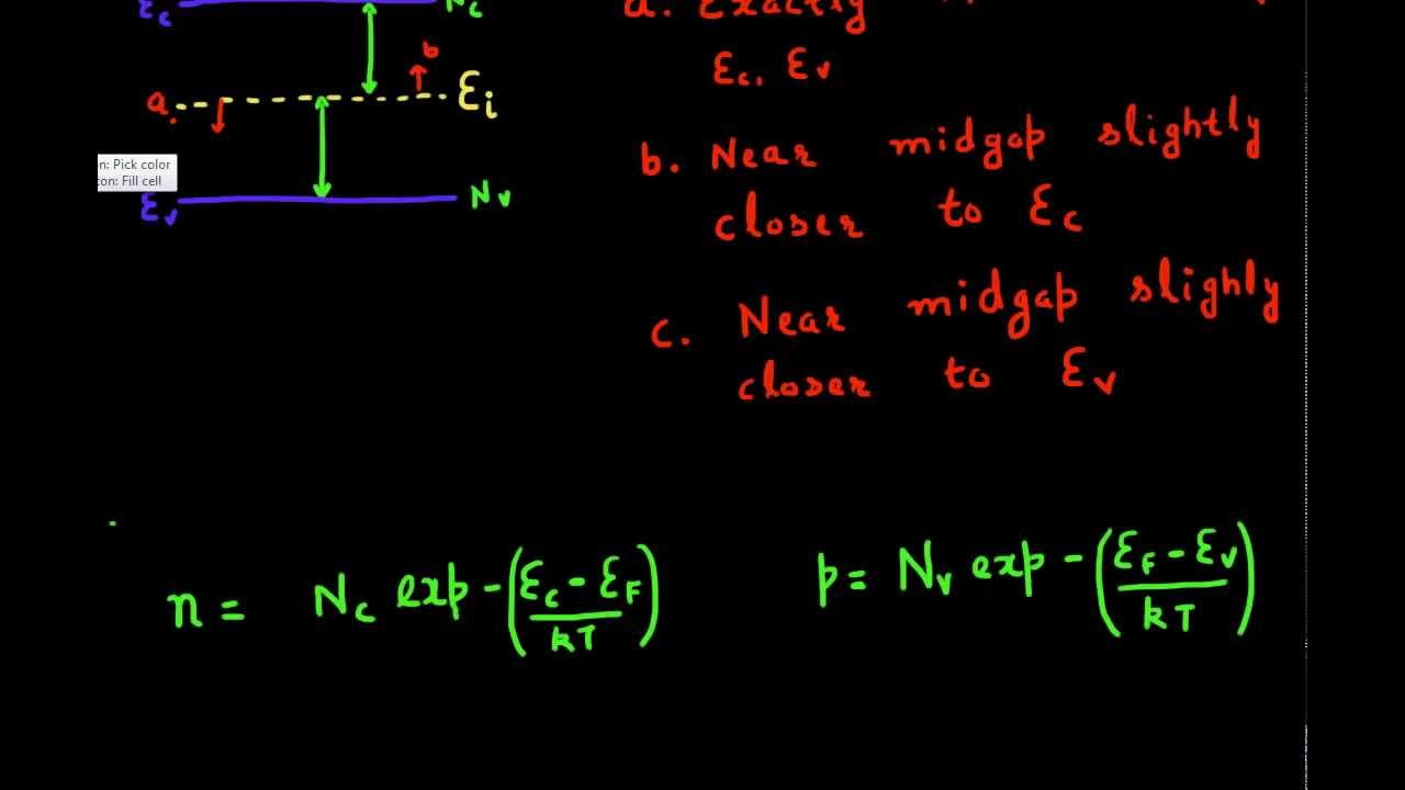
Find what part of germanium and silicon valence electrons is in the conduction band at temperature 300 k. Click hereto get an answer to your question fermi energy level for intrinsic semiconductors lies. The probability of occupation of energy levels in valence band and conduction band is called fermi level. By electrically tuning the fermi level in graphene, it is possible to change its optical absorption in a broad range of as intrinsic electron (hole) density is usually low at room temperature, carrier density of a typical doped semiconductor is. Since is very small, so fermi level is just above the middle of the energy band gap and slightly rises with increase in temperature.
The Fermi level in intrinsic semi - conductors at toppr.com from d1hhj0t1vdqi7c.cloudfront.net Those semi conductors in which impurities are not present are known as intrinsic semiconductors. Hope it will help you. There is an equal number of holes and electrons in an intrinsic material. One is intrinsic semiconductor and other is extrinsic semiconductor. 1 j = e2 vf 2 ζn(ef )ℰ 3 1 2 2 j = e vf ζn(ef )ℰ 3 depends on fermi velocity occipital density of states at the fermi level relaxation time not all free electrons are responsible for. Differentiate between intrinsic semiconductors and intrinsic semiconductors? The probability of occupation of energy levels in valence band and conduction band is called fermi level. For intrinsic semiconductors like silicon and germanium, the fermi level is essentially halfway between the valence and conduction bands.
Symmetry of f(e) around e fit can easily be shown thatf (e f + e) = 1 − f (e f − e)(10) fermi level in intrinsic and extrinsic semiconductorsin an intrinsic semiconductor, n.
There is an equal number of holes and electrons in an intrinsic material. The number of charge carriers is therefore determined by the properties of the material itself instead of the amount of impurities. However as the temperature increases free electrons and holes gets generated. Hence, at 0k the valence band will be full of electrons while the conduction band will be empty (figure 2a). The pure form of the semiconductor is known as the intrinsic semiconductor and the semiconductor in which intentionally impurities is added for making it conductive is known as the extrinsic semiconductor. Intrinsic semiconductors in an intrinsic semiconductor, all the electrons in the conduction band are thermally excited from the valence band. The fermi level does not include the work required to remove the electron from wherever it came from. Extrinsic semiconductors are just intrinsic semiconductors that have been doped with impurity atoms (one dimensional substitutional defects in this considering that the fermi level is defined as the states below which all allowable energy states are filled and all states above are empty at the. Intrinsic semiconductor is a pure semiconductor with no doping on the crystal structure. It is a thermodynamic quantity usually denoted by µ or ef for brevity. Fermi level in an intrinsic semiconductor. Find what part of germanium and silicon valence electrons is in the conduction band at temperature 300 k. This level has equal probability of occupancy for the electrons as strictly speaking, fermi level locates not exactly at the middle of band gap of intrinsic semiconductors and there will always be a slight.